
3Dimension - News
3D PRINTING INDUSTRY REVIEW OF THE YEAR: OCTOBER 2020
October was an astronomical month for aerospace news, as NASA made significant progress in its preparation for the Artemis Moon mission, while printer manufacturer Zortrax worked with the ESA to develop space-age blended PEEK electronics.
![]()
NASA awarded several major contracts during October that could form part of its upcoming return to the Moon in Project Artemis. Image via ICON.
NASA projects take-off in run-up to Artemis
One of the biggest stories in October was the news that construction firm ICON had been awarded a NASA contract to develop an off-world AM system. During the project, codenamed ‘Olympus,’ ICON will work with the Marshall Space Flight Center to create a 3D printer that’s capable of turning lunar regolith into cosmic structures.
In another mission, Lockheed Martin was contracted by NASA to test its experimental cryogenic fuel systems, and the firm selected Relativity Space’s additive rockets to fire them into orbit. Relativity, which was chosen due to the flexibility of its process, is set to launch the potentially dangerous cargo in 2023.
NASA also awarded the University of North Dakota $750,000 in funding towards the development of its 3D printed NDX-3 spacesuit. The additive garment is set to be fabricated using a combination of flexible polymers over the next three years, before being compared to conventional flight suits via motion capture testing.
 Zortrax’s conductive new PEEK polymer could enable the creation of lighter, multifunctional parts. Photo via Zortrax.
Zortrax’s additive electronic advances
3D printed electronics made several strides forward during the month, starting with Zortrax and the ESA’s joint R&D project, which yielded prototype conductive PEEK filaments. Using their new materials, the team 3D printed multifunctional aerospace parts with data and electricity transfer capabilities.
Scientists from the University of New York at Buffalo and MIT, meanwhile, created a novel ferroelectric metamaterial for SLA 3D printing. According to the team, their composite resin could represent a step towards making synthetic materials more affordable within acoustic, shock absorbing and electronics applications.
Elsewhere, another MIT team developed a new 3D design environment that enables users to model both an object’s physical and electronic functions. Nicknamed the ‘MorphSensor,’ the program blends CAD and circuit building software together, to allow parts to be designed with optimal mechanical qualities.
 The U.S. Army worked with Wichita State University to create a digital twin of a Black Hawk helicopter (pictured) in October. Photo via Lockheed Martin.
The U.S. Army deploys 3D printing projects
The U.S. Army, which has a long tradition of leveraging additive technologies, embarked on a mission to 3D scan a 20,000-piece Black Hawk helicopter in October. In the teardown project, led by Wichita State University, the team developed a 3D printable catalog of all the aircraft’s components, allowing them to be reverse-engineered and optimized.
“We’ll evaluate every part, and not every part is necessarily going to be optimized for advanced additive manufacturing,” said Major General Todd Royar at the time. “But our intent is to literally go through all of our parts, starting with the UH-60, because those are the first ones we’ll have the 3D files for.”
Working with several U.S-based universities, the U.S. Army’s Research Laboratory also created a miniature 3D printed holographic instrument. The additive device proved capable of characterizing multiple airborne particles, and it could be deployed to identify potential aerosol threats to warfighters on the battlefield.
 Chiara Giusti created her FDM 3D printed TECHNĒ clothing line for her final university project at Politecnico di Milano. Photo via Chiara Giusti.
Fashionistas develop fabricated fashion lines
Textile 3D printing continued to gain traction in the fashion world, and Milanese designer Chiara Giusti exemplified this trend with her additive TECHNĒ clothing line. Developed alongside Superforma Fablab, the dresses were 3D printed using tension-activated TPUs, that could be both tailored to fit and comfortable to wear.
Similarly, London-based fashion designer Mingjing Lin completed her research into the potential of parametric modelling in October. According to Lin, fluidity in 3D printed textiles can be achieved using new modelling algorithms, such as those she previously deployed working with Sinterit to design an outfit for a Beijing Opera performance.
“I am proposing that fashion and textiles designers can embed our knowledge of complex body shape and body movement, as well as the sensibility of the tactile materials, into the application of these digital tools for creating intricate, fluid, and drapeable designs,” said Lin.
To stay up to date with the latest 3D printing news, don’t forget to subscribe to the 3D Printing Industry newsletter or follow us on Twitter or liking our page on Facebook.
Are you looking for a job in the additive manufacturing industry? Visit 3D Printing Jobs for a selection of roles in the industry.
Featured image shows a concept image of what ICON’s 3D printed off-world structures could look like. Image via ICON.
Researchers Model and 3D Print Graphene Electronic Devices
November 16, 2020by Michael Molitch-Hou3D Printing3D Printing Materials3D Printing Research

Made up of single atoms of carbon, graphene is thought to be a wonder material with a wide variety of applications, due to its high strength, lightweight, flexibility and unprecedented electrical conductivity. However, producing large graphene parts at scale remains a challenge. Previous research has shown that various methods for 3D printing graphene exist, but these techniques are still limited in size. Moreover, both these processes and non-additive methods for the production of large-area graphene layers hinder some of desired characteristics of the material, namely electrical conductivity.
Now, researchers at the University of Nottingham have developed a technique for 3D printing graphene using an inkjet technology that maintains the materials electrical properties, opening up possibilities for an array of electronic components, such as transistors and sensors. The study, titled “Inter-Flake Quantum Transport of Electrons and Holes in Inkjet-Printed Graphene Devices”, is published in the journal Advanced Functional Materials.
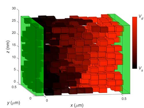
![]()
A 3D-printed phototransistor made up of “an exfoliated InSe flake contacted with six inkjet‐printed graphene stripes (each comprising 5 printed layers, 7 lines), which serve as electrodes, on a 300 nm SiO2/Si substrate.”
As a two-dimensional material, graphene is usually made by exfoliating individual layers of carob atoms in the form of a flat sheet. To then craft a multi-layer object of this material then requires hand-deposition of these sheets, an obviously laborious process. To fully exploit the properties of this wonder material through a scalable process, the University of Nottingham team developed a method for inkjetting inks loaded with flakes of graphene. Moreover, through the use of quantum mechanical modeling, the researchers are able to understand exactly how electrons move through the layers of graphene in order to control the electrical properties of the printed material.
Professor Mark Fromhold, Head of the School of Physics and Astronomy and a co-author on the paper, put it this way:
“By linking together fundamental concepts in quantum physics with state-of-the art-engineering, we have shown how complex devices for controlling electricity and light can be made by printing layers of material that are just a few atoms thick but centimeters across. According to the laws of quantum mechanics, in which the electrons act as waves rather than particles, we found electrons in 2D materials travel along complex trajectories between multiple flakes. It appears as if the electrons hop from one flake to another like a frog hopping between overlapping lily pads on the surface of a pond.”
To print the material, graphene inks made up of graphene flakes and ethyl cellulose, were dispersed into a mixture of cyclohexanone/terpineol and printed onto a substrate using a drop-on-demand method. The layers were then annealed in a vacuum oven at 250°C to remove the solvent and breakdown the additives within the ink. The team found that the greater the number of layers, the lower the electrical resistance. To demonstrate the possibilities of the material, the team 3D printed a phototransistor made up of graphene electrodes printed onto a semiconducting crystal.
A simulation of packed graphene flakes between two contacts.
Key to the research was understanding the movement of electrons in order to best produce graphene parts. To do this, the team modeled the conductive properties of the network of flakes within the printed parts, simulating the charge transfer between flakes of graphene as virtual voltage is applied to a simulated device. The authors note: “Our model reveals the mechanism of carrier transport in printed graphene layers and shows that optimized thickness of printed layers with high [packing fraction] is required to achieve high conductivity devices.”
To understand how printed graphene would work within a device made of multiple types of materials, the researchers 3D printed a field-effect transistor. The electrical resistance was actually higher than expected for five printed layers of graphene due to the mixing of inks between layers.
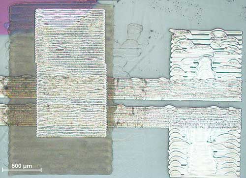
Optical microscopy image of the 3D printed graphene field-effect transistor; “scale bar is 500 µm, spacing between silver electrodes is 100 µm.”
Co-author, Dr Lyudmila Turyanska from the Centre for Additive Manufacturing, said of the work:
“While 2D layers and devices have been 3D printed before, this is the first time anyone has identified how electrons move through them and demonstrated potential uses for the combined, printed layers. Our results could lead to diverse applications for inkjet-printed graphene-polymer composites and a range of other 2D materials. The findings could be employed to make a new generation of functional optoelectronic devices; for example, large and efficient solar cells; wearable, flexible electronics that are powered by sunlight or the motion of the wearer; perhaps even printed computers.”
Next, the team plans to refine the deposition of the graphene through the use of polymers in order to impact the way that flakes align. They also hope to use different types of inks with varying sizes of graphene flakes. The researchers will also improve their computer simulations to include how the different materials work together. Finally, they aim to develop methods for mass production of the prototyped devices.
Tagged with: 3d printed electronics • 3d printed graphene • 3d printing materials • 3d printing research • nottingham • university of nottingham
Multimaterial 4D Printing with Tailorable Shape Memory Polymers
Abstract
We present a new 4D printing approach that can create high resolution (up to a few microns), multimaterial shape memory polymer (SMP) architectures. The approach is based on high resolution projection microstereolithography (PμSL) and uses a family of photo-curable methacrylate based copolymer networks. We designed the constituents and compositions to exhibit desired thermomechanical behavior (including rubbery modulus, glass transition temperature and failure strain which is more than 300% and larger than any existing printable materials) to enable controlled shape memory behavior. We used a high resolution, high contrast digital micro display to ensure high resolution of photo-curing methacrylate based SMPs that requires higher exposure energy than more common acrylate based polymers. An automated material exchange process enables the manufacture of 3D composite architectures from multiple photo-curable SMPs. In order to understand the behavior of the 3D composite microarchitectures, we carry out high fidelity computational simulations of their complex nonlinear, time-dependent behavior and study important design considerations including local deformation, shape fixity and free recovery rate. Simulations are in good agreement with experiments for a series of single and multimaterial components and can be used to facilitate the design of SMP 3D structures.
Introduction
Three-dimension (3D) printing technology allows the creation of complex geometries with precisely prescribed microarchitectures that enable new functionality or improved and even optimal performance. While 3D printing has largely emphasized manufacturing with a single material, recent advances in multimaterial printing enable the creation of heterogeneous structures or composites that have myriad scientific and technological applications1,2,3,4,5. Commercial printing systems with these capabilities have been used in many innovative applications, but are limited because their development has largely proceeded with objectives of creating printed components with reliable mechanical properties and applications have generally emphasized linear elastic behavior with small deformations where the innovation arises from the sophisticated geometry. Independently, soft active materials (SAMs) as a class of emerging materials with the capability of exhibiting large elastic deformation in response to environmental stimuli such as heat6,7, light8,9 and electricity10,11, are enabling the creation of functional active components. SAMs including shape memory polymers (SMPs), hydrogels, dielectric elastomers have been used to fabricate biomedical devices7,12,13, wearable devices14,15, artificial muscles10,11 and other smart products16,17,18. However, applications of SAMs are limited by the current manufacturing approaches which constrain active structures and devices to simple geometries, often created with a single material and they have yet to broadly exploit the potential of tailored microarchitectures.
This picture is changing as 3D printing and SAMs are being integrated. The most notable example is the recently developed “4D printing” technology2,3 in which the printed 3D structures are able to actively transform configurations over time in response to environmental stimuli. There are two types of SAMs mainly used to realize 4D printing: hydrogels that swell when solvent molecules diffuse into polymer network and shape memory polymers (SMPs) that are capable of fixing temporary shapes and recovering to the permanent shape upon heating. The examples of the hydrogel-based 4D printing include complex self-evolving structures actuated by multilayer joints5, active valves made of thermally sensitive hydrogel19, pattern transformation realized by heat-shrinkable polymer20 and biominic 4D printing achieved by anisotropic hydrogel composites with cellulose fibrils21. However, the low modulus of hydrogels ranging from ∼kPa to ∼100 kPa19,21 and the solvent diffusion based slow response rates in the time scale of a few ten minutes, hours and even days5,21,22 make the hydrogel based 4D printing not suitable for structural and actuation applications. Compared to hydrogels, SMPs have higher modulus ranging ∼MPa to ∼GPa7,23 and faster response rates (in the scale of seconds to minutes depending on actuation temperature)24,25. The examples of the SMP based 4D printing include printed active composites where precisely prescribed SMP fibers were used to activate the complex shape change2,3, sequential self-folding structured where SMP hinges with different responding rates were deliberately placed at different positions4 and multi-shape active composites where two SMP fibers with different glass transition temperatures26. To date, the SMP based 4D printing were mainly realized by commercial Polyjet 3D printer (Stratasys, Objet) which create materials with properties ranging between rigid and elastomeric by mixing the two base resins. The fact that users are not allowed to freely tune the thermomechanical properties beyond the realm of available resins impedes this 4D printing technology to advance to a wider range of applications. For example, the capability of 4D printed actuation is limited as the printed digital materials break at 10–25% 27; the printed structures could not be used in high temperature applications as the highest glass transition temperature of the available resin is about ∼70 °C4. In addition, this technology is not suitable for microscale applications as the lateral printing resolution is up to 200 μm inherently limited by the Polyjet printing method28.
In this paper we report a new approach that enables high resolution multimaterial 4D printing by printing highly tailorable SMPs on a projection microstereolithography (PμSL) based additive manufacturing system. We synthesize photo-curable methacrylate based copolymer networks using commercially-available materials. By tuning the material constituents and compositions, the flexibility of the methacrylate based copolymer networks enables highly tailorable SMP thermomechanical properties including rubbery modulus (from ∼MPa to ∼100 MPa), glass transition temperature (from ∼−50 °C to ∼180 °C) and the failure strain (up to ∼300%). Methacrylate based SMPs with different constituents or compositions form strong interface bonds with each other and enable fabrication of 3D structures made of multiple SMPs that can exhibit new functionality resulting from their dynamic thermomechanical properties. The PμSL based additive manufacturing system with high lateral resolution up to ∼1 μm exploits a digital micro-display device as a dynamic photo mask to dynamically generate and reconfigure light patterns, which then converts liquid monomer resin into solid via photo-polymerization in a layer-by-layer fashion29,30,31. A high resolution, high contrast digital micro-display device ensures high resolution structure made of methacrylate based SMPs that require higher exposure energy than acrylate based polymers which have been frequently used for 3D printing but do not have SM effect. Multimaterial manufacturing is achieved via an automatic material exchanging mechanism integrated into the PμSL additive manufacturing system. In addition, a highly fidelity computational tool based on the understanding of the shape memory behavior is used to facilitate the design of SMP 3D structures by simulating important design considerations including local deformation, shape fixity and free recovery rate. We believe this novel approach will translate the SMP based 4D printing into a wide variety of practical applications, including biomedical devices12,13,32,33, deployable aerospace structures34,35, shopping bags36,37 and shape changing photovoltaic solar cells38,39.
Results
Multimaterial additive manufacturing system
We fabricate high resolution multimaterial shape memory structures on an additive manufacturing apparatus based on projection microstereolithography (PμSL)29,30,31. As shown schematically in Fig. 1a, a computer aid design (CAD) model is first sliced into a series of closely spaced horizontal two-dimension (2D) digital images. Then, these 2D images are transmitted to a digital micro display which works as a dynamic photo-mask30. Ultraviolet (UV) light produced from a light emitting diode (LED) array is spatially modulated with the patterns of the corresponding 2D images and illuminated onto the surface of photo-curable polymer solution. Once the material in the exposed area is solidified to form a layer, the substrate on which the fabricated structure rests is lowered by a translational stage, followed by projection of the next image to polymerize a new layer on top of the preceding one. This process proceeds iteratively until the entire structure is fabricated. In the current setup, the projection area is about 3.2 cm × 2.4 cm resulting in a pixel size of ∼30 μm × 30 μm. The lateral resolution can be further improved up to as high as ∼1 μm if a projection lens with high optical magnification is used29. The step-and-repeat method can be employed to extend printing area without compromising lateral resolution30. Multimaterial fabrication is enabled by automating polymer solution exchange during the printing process. Although many efforts40,41,42 have been made to develop multimaterial fabrication systems by adding the automated polymer solution exchanging mechanisms into the “top-down” fabrication system (as shown schematically in Fig. 1a) where the modulated UV light projected downwards to the polymer resin, the multimaterial fabrication system developed based on the “bottom-up” approach making the depth of transparent polymer solution containers independent of the part height helps to significantly reduce material contamination and improve efficiency of material use43, but requires precise control of the oxygen concentration to separate the printed parts from the transparent polymer solution containers without damaging them43,44.
Figure 1
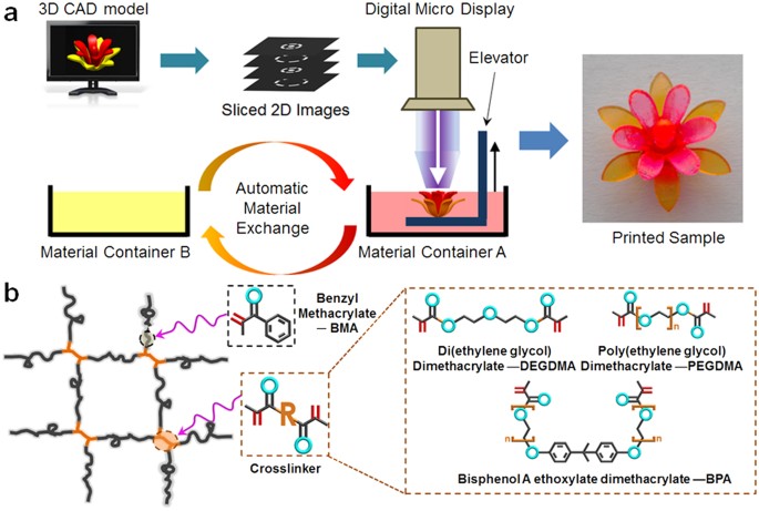
Schematics of multimaterial additive manufacture system.
(a) A workflow illustrates the process of fabricating a multimaterial structure based on PμSL (b) Photo-curable shape memory polymer network is constructed by mono-functional monomer, Benzyl methacrylate (BMA) as linear chain builder (LCB) and multi-functional oligomers, Poly (ethylene glycol) dimethacrylate (PEGDMA), Bisphenol A ethoxylate dimethacrylate (BPA) and Di(ethylene glycol) dimethacrylate (DEGDMA) as crosslinkers.
We fabricate shape memory structures using photo-curable methacrylate copolymers that form polymer networks via free radical photo-polymerization45,46,47. To understand the thermomechanical properties and shape memory (SM) effects of the materials and structures, we prepared polymer resins by using a mono-functional monomer, Benzyl methacrylate (BMA) as linear chain builder (LCB) and difunctional oligomers, Poly (ethylene glycol) dimethacrylate (PEGDMA), Bisphenol A ethoxylate dimethacrylate (BPA) and Di(ethylene glycol) dimethacrylate (DEGDMA) as crosslinkers that connect the linear chains to form a cross-linked network (shown in Fig. 1b). Details about polymer resin preparations can be founded in Methods. More selections of LCBs and crosslinkers are suggested by Safranski and Gall48.
Experimental Characterization
The photo-curable methacrylate networks provide high tailorability of thermomechanical properties of printed SMPs. Among them, the glass transition temperature (Tg), the rubbery modulus (Er) and the failure strain (εf) are the most critical properties for the design of active components as they dictate the shape recovery temperature and rate, constrained recovery stress and capability of shape change and/or actuation, respectively24,48,49,50,51. Figure 2a–c demonstrates that these thermomechanical properties can be tailored over wide ranges and still printed, by either controlling the concentration of crosslinker or using different crosslinkers. In Fig. 2a, for instance, for the copolymer network system consisting of BMA and crosslinker PEGDMA with molecular weight of 550 g/mole (denoted as B + P550), the Tg starts from ∼65 °C where the copolymer network system consists of pure BMA and then decreases with increase in the crosslinker concentration (See Supplementary Materials S1.1 I and Fig. S1a). The Tg of the copolymer networks consisting of the crosslinker PEGDMA with molecular weight of 750 g/mole (denoted as B + P750) and the crosslinker BPA with molecular weight of 1700 g/mole (denoted as B + BPA) follows the same trend of the B + P550 copolymer networks (Fig. S1b,c), while the Tg increases with increase in the crosslinker concentration of the copolymer network consisting of BMA and DEGDMA (denoted as B + DEG, Fig. S1d). The Couchman equation52 can be used to guide material design with a desired Tg by mixing the LCB and crosslinker with prescribed ratios: 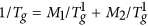 . Here,
  and
and  are the glass transition temperatures of the respective pure-components and M1 and M2 are the corresponding mass fractions. In Fig. 2a, using the current LCB monomer, namely BMA and crosslinkers, namely PEGDMA, BPA and DEGDMA allows us to adjust Tg from ∼−50 °C to ∼180 °C, while more flexibility can be obtained by choosing different LCB monomers and crosslinkers48 or even mixing more than one LCB monomers and crosslinkers to prepare the polymer resin53.
Figure 2
Experimental characterization of methacrylate SMP networks.
Highly tailorable glass transition temperature (a), rubbery modulus (b) and failure strain (c) are controlled by either changing the mixing LCB/crosslinker ratio or using different crosslinkers. (d) The temperature effect on the failure strain of the SMP consisting of 90% BMA and 10% BPA. (e) The normalized exposure energy to cure a thin layer varies with the crosslinker concentration as well as the molecular weight of crosslinker. (f) The investigation on the interface bonding of a printed composite with two components arranged in series (inset).
Figure 2b shows that the rubbery modulus Er of the copolymer networks increases with increase in crosslinker concentration (see Supplementary Materials S1.2, Fig. S2 and Table S1), as expected from entropic elasticity54, Er = (3ρRT)/Mc; here, R is the gas constant, T is absolute temperature, ρ is polymer density and Mc is average molecular weight between crosslinks. The ratio ρ/Mc is the crosslinking density of the polymer network which is affected by crosslinker concentration as well as the molecular weight of the crosslinker. Comparing the four network systems, the B + DEG network has the highest rubbery modulus at the same mass fraction of crosslinker, as the highest molar weight of DEGDMA leads to the highest crosslinking density (See Supplementary Materials S1.3 and Table S2) and the highest Er.
The effect of crosslinker on failure strain εf is shown in Fig. 2c; these results were obtained from uniaxial tensile tests at temperatures 30 °C above each sample’s Tg where sample stays the rubbery state to eliminate the effect of viscoelasticity (see Supplementary Materials S1.2, Fig. S2 and Table S1). The results shown in Fig. 2c suggest that in the SMP system consisting of the same LCB and crosslinker, the lower crosslinker concentration gives higher stretchability. Figure 2c also shows that the copolymer network system formed with a higher molecular weight crosslinker has higher stretchability. For example, for the copolymer systems consisting of 10% crosslinkers, the stretchability can be increased from ∼45% to ∼100% at 30 °C above sample’s Tg by increase the molecular weight from 242.3 g/mol (DEGDMA) to 1700 g/mol (BPA) (See Supplementary Materials S1.2, Fig. S2 and Table S1). Figure 2d shows the temperature effect on the failure strain of an SMP sample consisting of 90% BMP and 10% BPA (See Supplementary Materials S1.4 and Fig. S3). The stretchability of this copolymer network is increased by decreasing the stretching temperatures and finally reaches the maximum of ∼330% at 40 °C where the temperature is close to the peak of the loss modulus indicating the highest energy dissipation. A more stretchable network can be achieved by further reducing the crosslinker concentration of BPA or replacing BPA with a crosslinker having higher molecular weight.
Not only does the chemical composition affect the thermomechanical properties of the printed SMP systems, it also affects the photo-polymerization kinetics that determines the build rate during manufacturing. As shown in Fig. 2e, at a given UV light intensity, less exposure energy (time) is required to cure a layer of the same thickness when the crosslinker concentration increases (See Supplementary Materials S1.5 and Fig. S4a). This is mainly attributed to the reaction diffusion-controlled termination during the polymerization of the methacrylate based copolymer system55,56,57. With more crosslinker, the crosslinking density of the polymer increases, which limits the propagation of free radicals that would otherwise reach each other to terminate the polymerization57. Figure 2e also shows that the copolymer network consisting of a lower molecular weight crosslinker (P550) requires less exposure energy (time) to polymerize a same thickness layer. This is primarily because the low molecular weight crosslinker (P550) contains more unreacted double bonds per unit mass than the high molecular weight crosslinker (P750) does. In addition, the increase of photo initiator reduces the exposure energy (time) to cure a same thickness layer (See Supplementary Materials S1.5 and Fig. S4b). Moreover, it is necessary to note that under the same condition methacrylate based SMP has comparatively lower reactivity57 than those acrylate based materials such as poly(ethylene glycol) diacrylate (PEGDA) and hexanediol diacrylate which have been frequently used to print 3D structure29,30,31,44,58,59. This comparatively slow but conversion-dependent57 photo-polymerization kinetics makes the methacrylate based SMPs require higher (longer) exposure energy (time) to cure a layer of the same thickness than the acrylate based materials (See Supplementary Materials S1.5 and Fig. S4c). Therefore, a high contrast digital micro display with moderate intensity of UV light is needed to avoid any unwanted curing on the unintended parts (Details about the digital micro display are described in Materials).
In a printed component that consists of more than one material, the interface bonding between them significantly impacts the mechanical performance of the composite. In Fig. 2f, we investigated the interfacial bonding by uniaxially stretching a composite with two components arranged in series (Component A: 50% B + 50% P550 with Tg = 31 °C and Component B: 90% B + 10% BPA Tg = 56 °C) at a temperature 30 °C higher than Tg of Component B, where the both components are in their rubbery state (See Supplementary Materials S1.6 and Fig. S5). The fact that the composite breaks at Component A which has a lower failure strain rather than at the interface indicates a strong interface bonding. The comparison of uniaxial tensile tests between the composite and the two components in Fig. 2e reveals that Components A and B form a strong covalently boned interface through which the composite transfers stress completely between the two components. Generally speaking, this strong interface bonding forms between the methacrylate based SMPs made of different compositions and constitutes.
Shape Memory Behavior
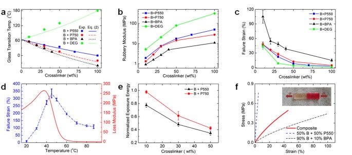
Two key attributes of SMPs are their ability to fix a temporary programmed shape (fixity) and to subsequently recover the original shape upon activation by a stimulus (recovery). Figure 3a shows a typical temperature-strain-time shape memory (SM) cycle that we used to investigate the fixity and recovery of SMP samples synthesized from different LCBs and crosslinkers that result in different Tg s. Figure 3b presents representative strain-time curves of a SMP strip sample made of 80% BMA + 20% P750. The SMP was first stretched to a target strain emax (20%) with a constant loading rate e (0.001 s−1) at a programming temperature TD (63 °C) and then the temperature was decreased to a TL (TL = 25 °C) with a cooling rate 2.5 °C/min. Once TL was reached, the specimen was held for 2 minutes and then the tensile force was removed. In the free recovery step, the temperature was increased to a recovery temperature TR (in Fig. 3b, TR = 35 °C, 40 °C, 50 °C and 60 °C, respectively) at the same rate of cooling and subsequently stabilized for another 20 min. (Details about the SM behavior testing are presented in Supplementary Material in S2.1 and Fig. S6).
Figure 3
SM behavior of the (meth)acrylate based copolymer SMP network.
(a) The SM behavior has been investigated by following a typical SM cycle: at Step I, a sample is deformed by emax at a programming temperature TD; at Step II, the temperature is decreased from TD to TL while keeping the sample deformed by emax; at Step III, after unloading, there is a deformation bounce back Δe; at Step IV, the free recovery is performed by heating the sample to a recovery temperature TR. (b) The representative SMP strain-time curves achieved by stretching a SMP sample (80% BMA and 20% P750) at 63 °C, unloading at 25 °C and heating to 63 °C, 50 °C, 40 °C and 35 °C, respectively. (c) Shape fixity as a function of programming temperature. (d) Shape recovery time (t0.95) as a function of recovery temperature.
As shown in Fig. 3a,b, we use the small strain bounce back, Δe, of the SMP after unloading to define the shape fixity, i.e., Rf = (emax − Δe)/emax. Figure 3c shows that the shape fixity is a function of the programming temperature TD (Details about TD are listed in Supplementary Material Table S4): the SMP keeps a high shape fixity (>90%) when TD is above or near the SMP’s Tg and the shape fixity starts to drop dramatically when TD is 20 °C lower than the SMP’s Tg. The phenomenon that the shape fixity is a function of TD agrees the previous study24 and can be simulated by the recently developed multi-branch model which consists of an equilibrium branch corresponding to entropic elasticity and several thermoviscoelastic nonequilibrium branches to represent the multiple relaxation processes of the polymer24,60 (Details about the multi-branch model are presented in Supplementary Material S2.2–2.3). The model predictions agree with the experiments well and provide underlying understanding of the effect of the programming temperature TD on the shape fixity Rf (Details about model predictions are presented in Supplementary Material S2.4 and Figure S9). When TD is higher or near the Tg, an SMP has a high shape fixity Rf, as the time requires to relax all the nonequilibrium stresses is shorter than the time used for loading at TD and cooling to TL. When TD is decreased to a lower temperature the shape fixity Rf decreases as the nonequilibrium stresses do not have sufficient time to relax. For example, in Fig. 3c, the simulation indicates that for the SMP of 90% BMA + 10% BPA with Tg = 56 °C, Rf is decreased to nearly zero when TD is 25 °C where the polymer chain mobility is significantly reduced and the unrelaxed nonequilibrium stresses are stored as elastic energy.
Figure 3d indicates that the free shape recovery is a function of recovery temperature (Details about how to achieve the free recovery curve are presented in S2.1). We define the shape recovery ratio as Rr = 1−e(t)/(emax−Δe). We use the recovery time t0.95 that corresponds to a 95% shape recovery ratio to measure the shape recovery rate at different recovery temperatures TR24. Within the lab scale experiment time (an hour), the SMP samples were able to realize the 95% shape recovery only at the recovery temperature TR more than 10 °C higher than the SMP’s Tg (the measured t0.95 are listed in Table S5). The multi-branch model is also used to simulate the free recovery at different recovery temperatures TR and predict the recovery time t0.95 at different TR s (See Supplementary Material S2.4). Overall, t0.95 increases exponentially with a decreasing TR and for different SMPs, at the same TR, the one with a higher Tg requires a longer recovery time.
Three dimensional printed structures with a single SMP
Figure 4 shows the ability of our additive manufacturing system to create complex 3D structures that exhibit nonlinear large deformation SM behavior. As shown in Fig. 4aI, a spring was fabricated using a SMP with Tg = 43 °C (80% B + 20% P750). We demonstrated the SM effect of the spring by stretching it to a straight strand at 60 °C. The straight strand configuration was fixed (Fig. 4aII) after removing the external load at 20 °C. It recovered the original spring shape (Fig. 4aII–V) after heating back to 60 °C. The complicated nonlinear large deformation SM behavior of the spring was investigated by following the typical SM cycle for a spring with a representative segment (See Supplementary Material S3.3). Figure 4b shows the force-displacement relation when the spring was stretched at 60 °C. The spring becomes extremely stiff as it approaches to its fully unfolded state. The finite element (FE) simulations present the deformation contours in the progress of stretching the spring. Regardless of the maximum deformation on the two ends, the highest principle engineering strain on the main body of the spring was in the range from 70–100% which is about two to three times higher than the failure strain of previously reported SMPs used for 4D printing2, indicating the enhanced mechanical performance which is a necessity for active structures. In “4D printing” where the fourth dimension is “time”, a key desire is to control of the actuation rate. For the printed shape memory structures, the actuation rate can be controlled by the recovery temperature24,49. Figure 4c shows the recovery ratio of the stretched spring at different recovery temperatures. Here, the recovery ratio of the SM spring is defined as  , where d(t) is the end-to-end displacement during heating, dmax is the maximum displacement before unloading at 20 °C and Δd is the bounce back displacement after unloading. As seen in Fig. 4c,
  is highly dependent on the recovery temperature. At 60 °C, the spring was fully recovered into the initial shape within 3 mins. The recovery rate was significantly slower at 35 °C where only about 10% recovery took place after 20 mins holding. The SM behavior including the free recovery at different temperatures of the 3D printed spring can be simulated by implementing the multi-branch model into FE software ABAQUS (Simulia, Providence, RI, USA). In Fig. 4c, the FE simulation reproduced the free recovery behavior at different recovery temperatures, indicating that the multi-branch model can be used to design complex 4D printed structures that are made of SMPs and exhibit complex nonlinear large deformation thermomechanical behaviors. Details about FE simulation of SM behavior of this printed spring are described in Supplementary Material S3.3 and Supplementary Movies 1a–d.
Figure 4
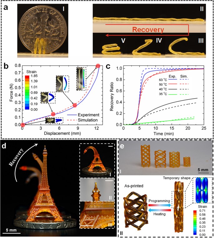
3D printed shape memory structures with single material.
(a) A 3D printed shape memory spring (I) was programmed to a straight strand temporary configuration (II) and then recovered to its original shape upon heating (III–V). (b) Experimental characterization and FE simulation were performed to investigate the nonlinear deformation. (c) Experiments and simulations of the free recovery at different temperatures. (d) 3D printed SM Eiffel tower. (e) 3D printed SM stents.
Figure 4d shows a more refined and complex 3D printed structure Eiffel Tower standing on a Singapore dollar. It was printed with the SMP made of 80% B + 20% P750 too. Following the SM cycle, a temporary bent shape (Fig. 4dI) was achieved by bending the Eiffel tower at 60 °C and removing the external load after cooling to 25 °C. After heating back to 60 °C, the bent Eiffel tower gradually recovered its original straight shape (Fig. 4d, Supplementary Movie 2). Figure 4e demonstrates one of the most notable applications of SMPs — cardiovascular stent. Although there have been various efforts directed at fabrication12,32, material and structural characterization12,61,62 and simulations32,63,64,65, the design of the stents has been limited primarily by fabrication methods because traditional manufacturing approaches are usually complex, consisting of multiple time-consuming steps, to achieve the geometric complexity and resolution necessary for stents12,32. Our additive manufacturing system offers the ability to fabricate high resolution 3D shape memory structures with hardly any restriction of geometric complexity. Figure 4eI shows an array of stents printed in one batch with different geometric parameters including the height and the diameter of a stent, the number of joints, the diameter of ligaments and the angle between ligaments. In Fig. 4eII, a 3D printed stent was programmed into the temporary shape with a smaller diameter for minimally invasive surgery. After heating, the stent was recovered into the original shape with a larger diameter used to expand a narrowed artery. The finite element (FE) simulation shown in Fig. 4eII gives an insight into the local large deformation that occurs in the temporary shape and renders existing additive manufacturing systems and materials infeasible. The simulations provide a guide for the material selection based on the understanding of the thermomechanical properties from Fig. 2.
Three dimensional printed structures with multiple SMPs
Figure 5 demonstrates the printing of a 3D printed structure with multiple SMPs - multimaterial grippers that have the potential to function as microgrippers13 that can grab objects, or drug delivery devices33,66 that can release objects. Figure 5aI shows a number of multimaterial grippers with different designs including different sizes and numbers of digits (comparing